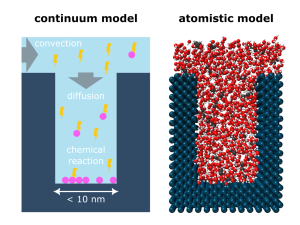
The miniaturization of semiconductor technology has led to fabrication processes at extremely small length scales. State-of-the-art integrated circuits are manufactured via patterned nano-size holes in silicon wafers that are exposed to wet cleaning during the numerous production steps. Liquid transport at the nano-scale, and hence the cleaning process, can no longer be described by classic continuum theories as interactions between the constituting molecules become relevant. Besides the physico-chemical properties of the fluid, the ongoing chemical reactions inside the nano-holes further affect the molecular transport.
In this project, to describe transport in chemically active nano-confinement, we employ atomistic modelling techniques, especially focusing on molecular dynamics simulations. The major goal is to understand the diffusion mechanism of (multi-component) liquids in the bulk and confined spaces and how channel size, shape and wetting affect their transport behavior. We further investigate how an atomistic nano-hole model can be coupled to a continuum model for the liquid transport on top of the wafer.