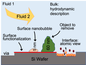
Semiconductors are essential for electronic devices. They are assembled onto silicon wafers, and their efficiency is related to the level of cleanness of their exposed interface. The continuous trend toward miniaturization of electronic components, require novel solutions to clean wafer surfaces from particles that are in the nanometer scale ( [<] 200 nm in radius). Recently, it has been proved that localized surface nanobubbles created via water-solvent exchange, can improve the removal of particles efficiency. Nevertheless, the process is still not well understood.
This work, aims to clarify the nature of surface nanobubble formation and activity on particles. By using atomic force microscopy (AFM) with an ad hoc cell design, we aim to observe the formation of surface nanobubbles and describe their dynamics in different environmental conditions (temperature, solvents), substrate wettability (hydrophobic or –philic), and interaction with particles of different sizes and types.

